By Team MEG
India’s semiconductor ambitions are usually discussed through the lens of wafer fabs. But assembly, testing and increasingly advanced packaging are beginning to create manufacturing capacity sooner—and may provide the country with its first large operating semiconductor ecosystem.
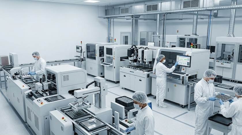
Hero visual: semiconductor assembly, packaging and test as precision industrial manufacturing.
The Signal
India’s semiconductor push is beginning to move from project announcements into actual production. Micron opened its semiconductor assembly and test facility at Sanand in February 2026. Kaynes Semicon began production at its Sanand plant in March. In July, CG Semi’s OSAT facility also entered commercial production. Packaging and test are therefore among the semiconductor projects moving fastest from approval to operating manufacturing capacity.
At the same time, India is pursuing the much harder task of establishing front-end wafer fabrication. Tata Semiconductor Manufacturing’s Dholera project, planned at roughly ₹91,000 crore and 50,000 wafer starts per month, is intended to become India’s first major commercial semiconductor fab.
The distinction matters. A semiconductor does not become a usable chip when the wafer leaves the fab. Individual dies must still be separated, connected, protected and tested before they can enter an automobile, inverter, telecom system or consumer device. That back-end manufacturing layer is where India may build scale first.
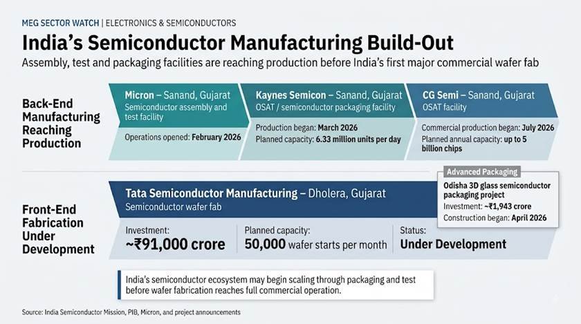
Visual 1: India’s semiconductor manufacturing build-out — back-end facilities are reaching production while front-end fabrication remains under development.
Why Packaging Can Move Earlier
Wafer fabrication is one of the most demanding manufacturing activities in the world. A modern fab requires enormous capital expenditure, specialised process equipment, ultra-clean manufacturing environments, advanced materials and gases, extremely stable utilities, high process yields and deep operating experience.
Assembly, testing and packaging remain technically demanding, but the entry conditions are different. They allow India to participate further downstream in semiconductor manufacturing without first reproducing every capability required for advanced wafer fabrication.
Micron expects its Sanand facility to assemble and test tens of millions of chips during 2026 before scaling further in 2027. Kaynes’ facility is designed to reach approximately 6.33 million units per day across its completed phases, beginning with advanced Intelligent Power Modules for automotive and industrial applications. CG Semi’s Sanand operation is expected to scale toward an annual capacity of up to 5 billion semiconductor chips.
These are not substitute fabs. They are a different layer of the semiconductor value chain—and one that can begin creating operating experience, supplier relationships, skilled manpower and quality systems while India’s front-end fabrication capability is still developing.
Packaging Is Also Becoming More Strategic
The word packaging can sound deceptively simple. Historically, packaging primarily protected the semiconductor die and connected it electrically to the outside world. But advanced computing is making package architecture increasingly important to performance.
Modern packaging can combine multiple dies, interposers, substrates and specialised connections into increasingly sophisticated systems. In April 2026, construction began in Odisha on a roughly ₹1,943 crore advanced 3D glass semiconductor packaging facility. The project is planned to manufacture glass substrates, assembled devices and 3D heterogeneous-integration modules for applications including AI, high-performance computing, defence electronics, telecom and data centres.
That changes the industrial proposition. India is not only trying to become a location for conventional assembly. It is beginning to pursue parts of the higher-value packaging technology stack as well.
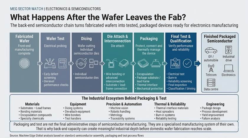
Visual 2: the semiconductor back-end chain — packaging and test form a specialised manufacturing system of their own.
The Industrial Ecosystem Behind the Package
Packaging materials: Substrates, lead frames, bonding materials, encapsulation compounds and specialty chemicals.
Precision equipment: Dicing systems, die-attach equipment, wire bonders, moulding systems, inspection and test handlers.
Thermal engineering: Heat spreaders, interface materials and increasingly sophisticated package-level thermal management.
Testing: Electrical testing, reliability screening, burn-in and failure analysis.
Automation and metrology: Machine vision, precision handling, clean manufacturing equipment and traceability systems.
Engineering capability: Package design, process development, yield improvement and reliability engineering.
This is where the semiconductor story begins to intersect strongly with India’s existing industrial capabilities in electronics manufacturing, precision engineering, automation and engineering services. The opportunity is therefore broader than simply counting packaged chips. It is the possibility of building a domestic back-end semiconductor manufacturing cluster around the facilities entering operation.
The India Angle
India’s fab ambitions remain strategically important. Without wafer fabrication, the country will still depend heavily on overseas front-end manufacturing for many devices. But semiconductor ecosystems rarely appear fully formed.
Packaging and test provide India with a route to begin accumulating manufacturing capability now: process discipline, cleanroom operations, semiconductor quality systems, specialised logistics, trained technicians, equipment servicing and supplier development.
Because these facilities are already reaching production while large-scale fab capacity is still being built, they may become the first practical training ground for India’s semiconductor manufacturing ecosystem.
What MEG Is Watching
| Production ramp-up | Advanced packaging | Domestic supplier depth | Fab-to-package integration |
| Whether recently inaugurated OSAT and ATMP facilities move rapidly from initial output to sustained commercial scale. | Whether early 3D and heterogeneous-integration projects develop into genuine high-value capability rather than isolated projects. | How much packaging material, equipment support, automation and testing capability begins to localise around these plants. | When Indian-fabricated wafers begin flowing into Indian packaging and test facilities, creating a connected domestic semiconductor chain. |
India’s semiconductor ambition will ultimately be judged across the entire value chain. But the first large manufacturing layer to become visible may not be the fab.
It may be what happens after the wafer is made.
Sources & Further Reading
• Micron: Opening of the Sanand semiconductor assembly and test facility, February 2026.
• Press Information Bureau / India Semiconductor Mission: Tata Semiconductor Manufacturing Dholera fab project and approved semiconductor projects.
• Press Information Bureau: Kaynes Semicon production and planned capacity at Sanand.
• Press Information Bureau: CG Semi commercial production and capacity at Sanand.
• Press Information Bureau: Odisha 3D glass semiconductor packaging project, construction begun April 2026.